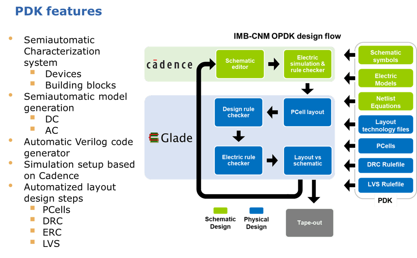
The IMB-CNM Organic Process Design Kit (OPDK) offers a fast automatic methodology for characterization, modelling and simulation of electronic devices and basic building blocks for multiple technologies. The layout automatization is implemented through PCells and the quality checked with DRC, ERC and LVS, providing a semi-automatic PDK for state-of-the-art organic and printed electronics.
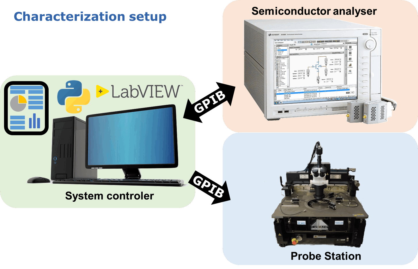
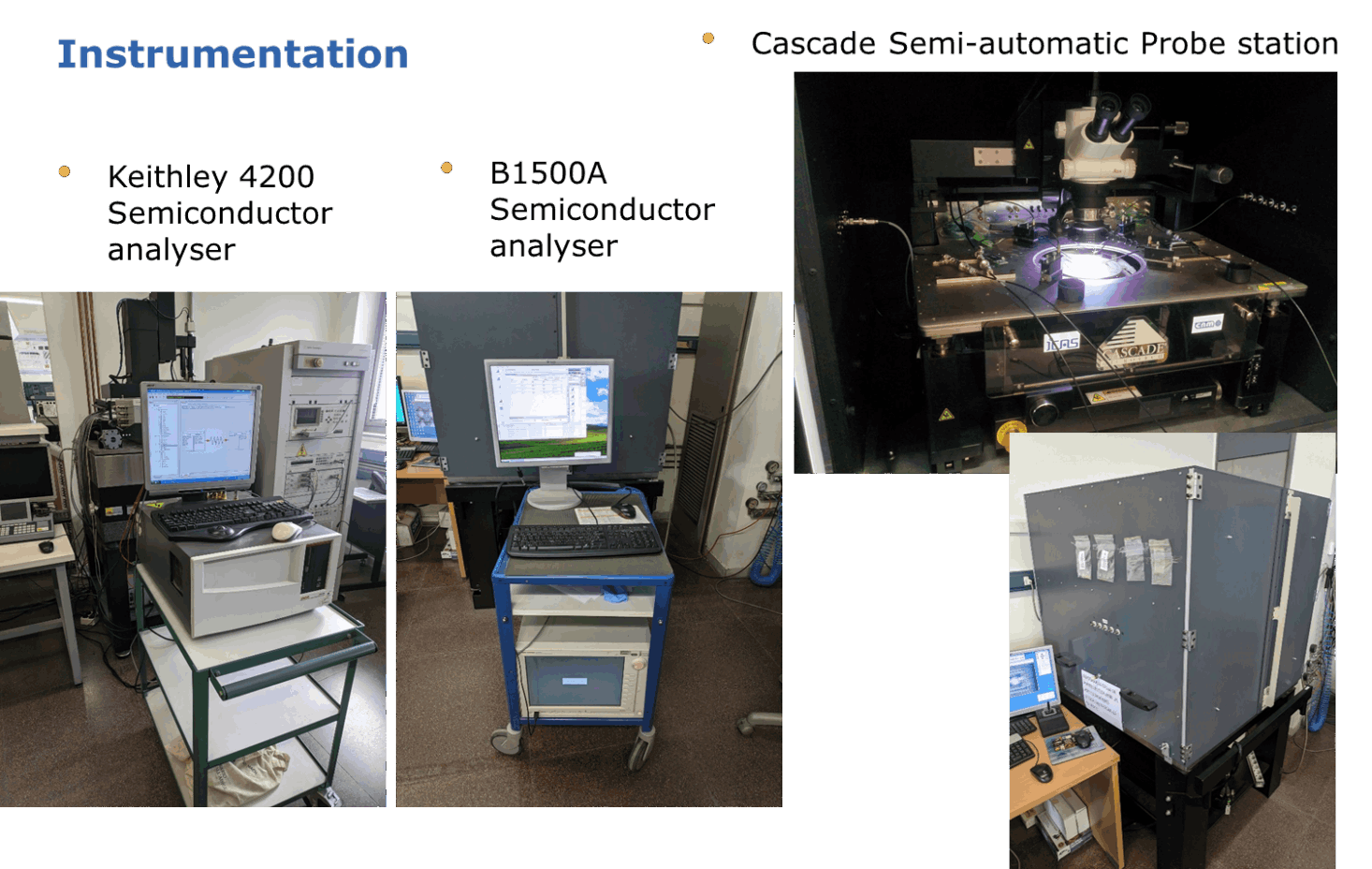
IMB-CNM OPDK is automatized with Python scripts, which allow high adaptability to new technologies, devices and basic building blocks in the setup. The system controller coordinates the instruments involved, which comprise the semiconductor analyser (Agilent B1500A or Keithley 4200) and the semi-automatic probe station (Cascade Microtech SUMMIT 12161B-6). Additionally, the system controller acquires the test results and generates a final report with all the data and statistical parameter analysis. System control is carried out through the VISA protocol in a GPIB connection, allowing fast and reliable data transmission.
Device characterization
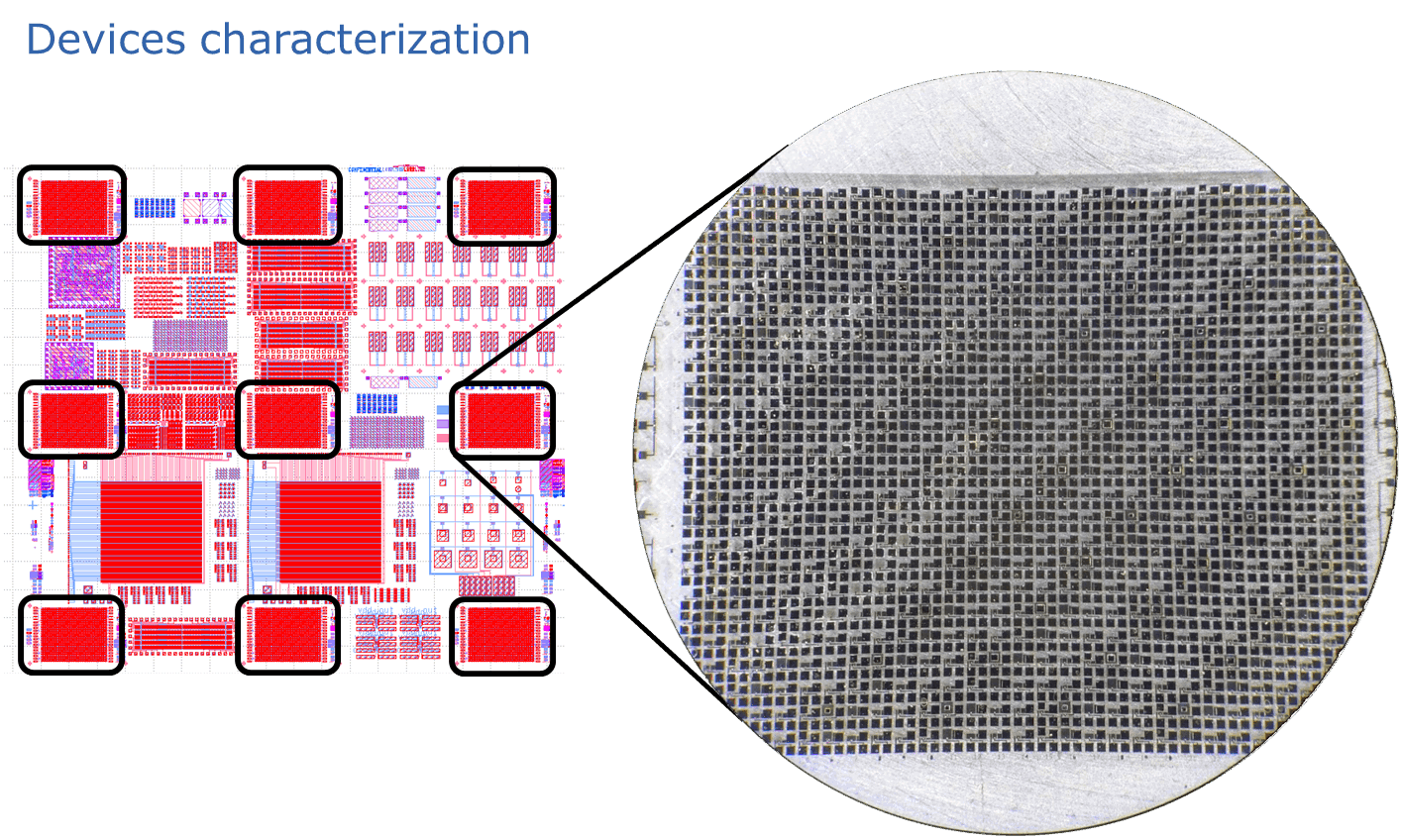
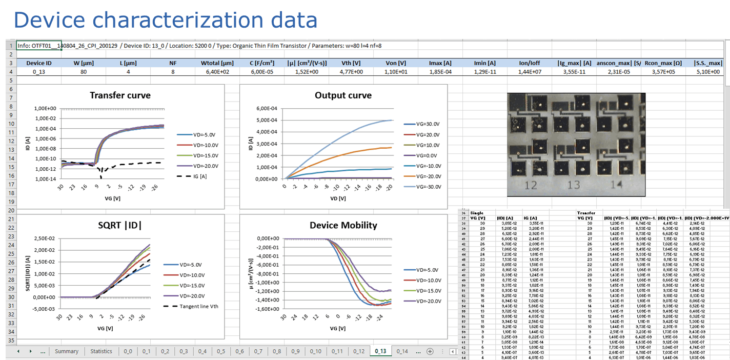
To date, IMB-CNM OPDK has been used to characterize more than 6000 OTFTs manufactured by lithography and 15.000 OTFTs inkjet-printed, localized in arrays from 695 up to 1.000 devices. Using the automatic setup, OPDK allows extraction of all data and analysis of interesting device parameters for modelling purposes.
Transfer and input curves for specified voltages are extracted for each device. Furthermore, key parameters are calculated such as capacitance per unit area, device mobility, threshold voltage, turn on voltage, maximum current, minimum current, maximum/minimum current ration, maximum gate current, maximum transconductance, maximum connection resistance and maximum sub-threshold swing. Position maps are also generated allowing identification of the different devices. Global statistical data is extracted allowing a quick overview of how the characterization of the run parameters and evaluation of the devices can be performed.
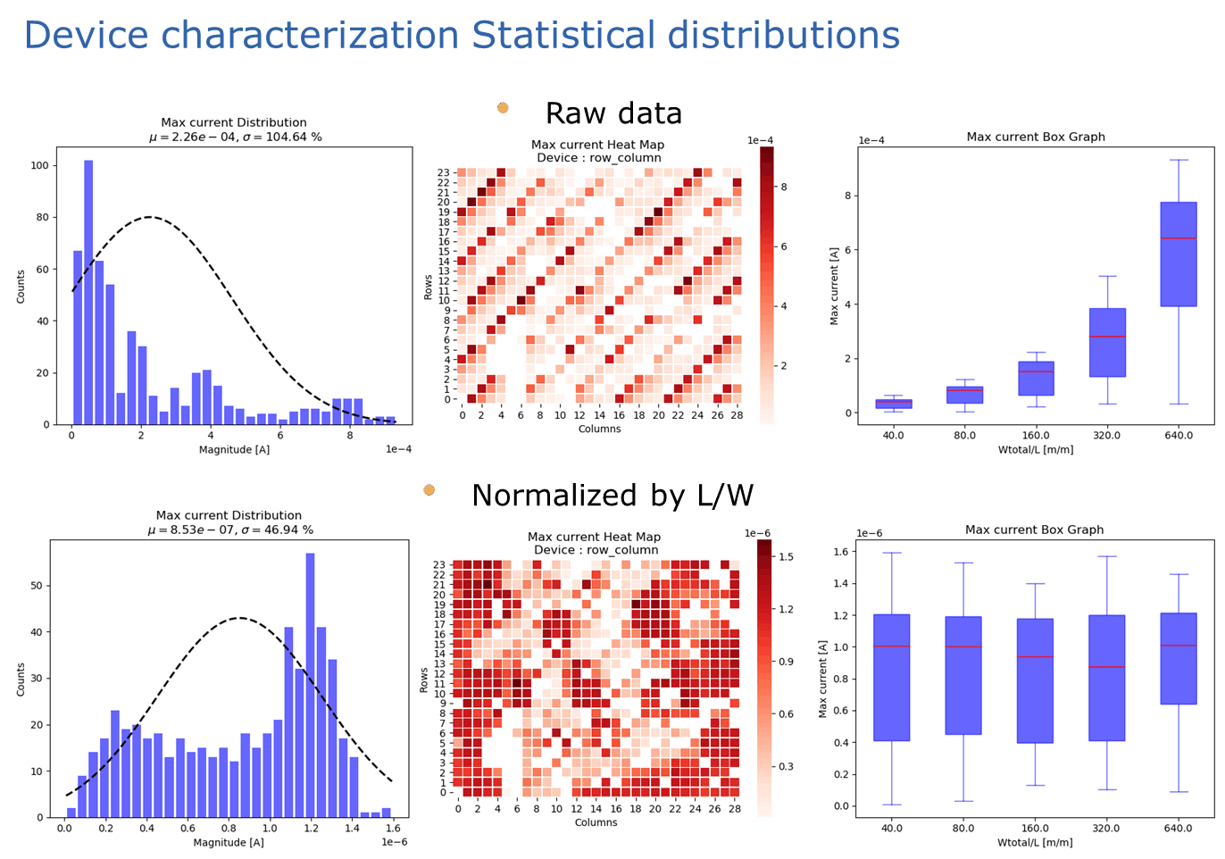
Tendencies in sizes and run positions are identified via calculation of statistical distributions of key parameters such as device mobility, threshold voltage, turn-on voltage, maximum current, minimum current, maximum/minimum current ratio, maximum gate current, maximum transconductance, maximum connection resistance and maximum sub-threshold swing. Furthermore, the statistical report includes raw data of non-normalized devices and data of normalized devices allowing a study of the best geometry ratio.
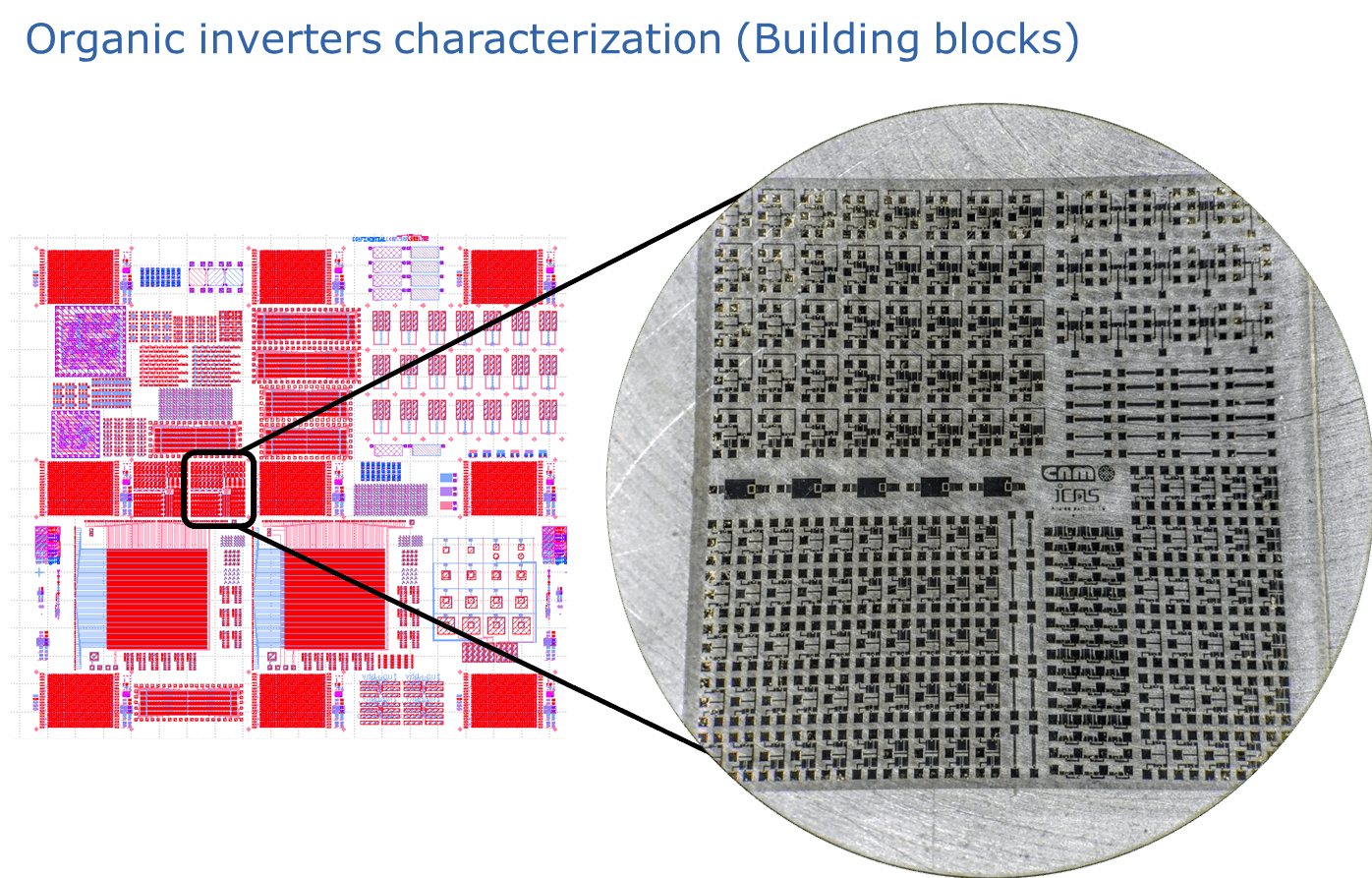
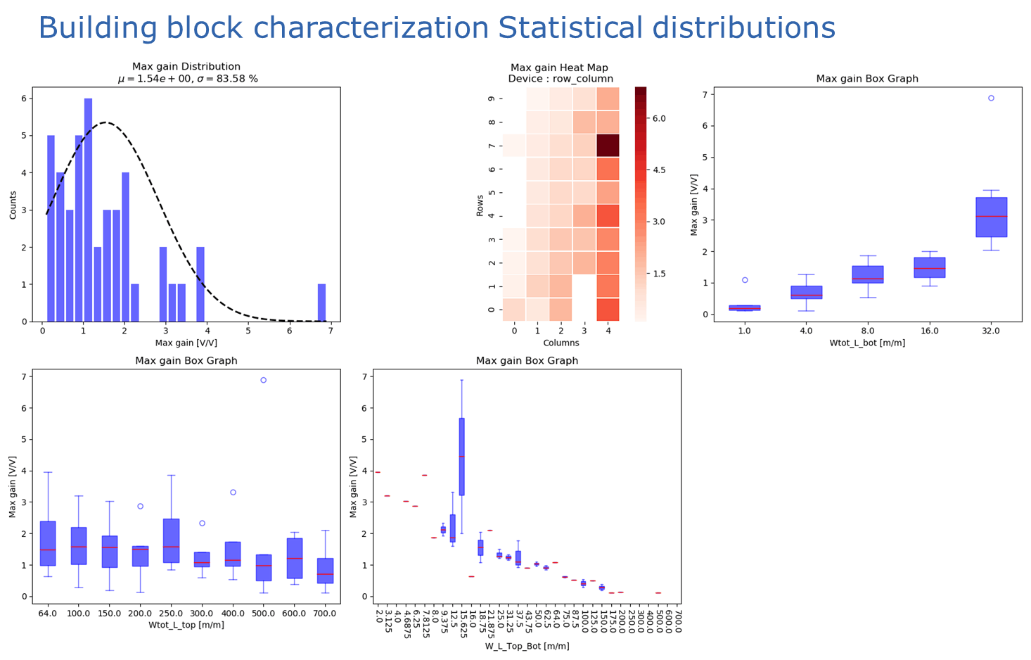
The methodology for characterising devices can also be used for basic building blocks. In this case, the characterization is done on inverters, but the setup can be adapted to any circuit of up to 6 source or measure points (SMU).
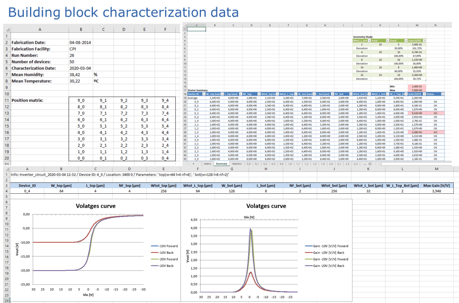
A position matrix is generated for basic building block identification. Global statistics are also extracted and the data of each circuit is represented by graphs. Key parameters are also obtained i.e. maximum gain in the case of an inverter.
Statistical distributions of key parameters such as gain are calculate to allow identification of tendencies in size and run positions.
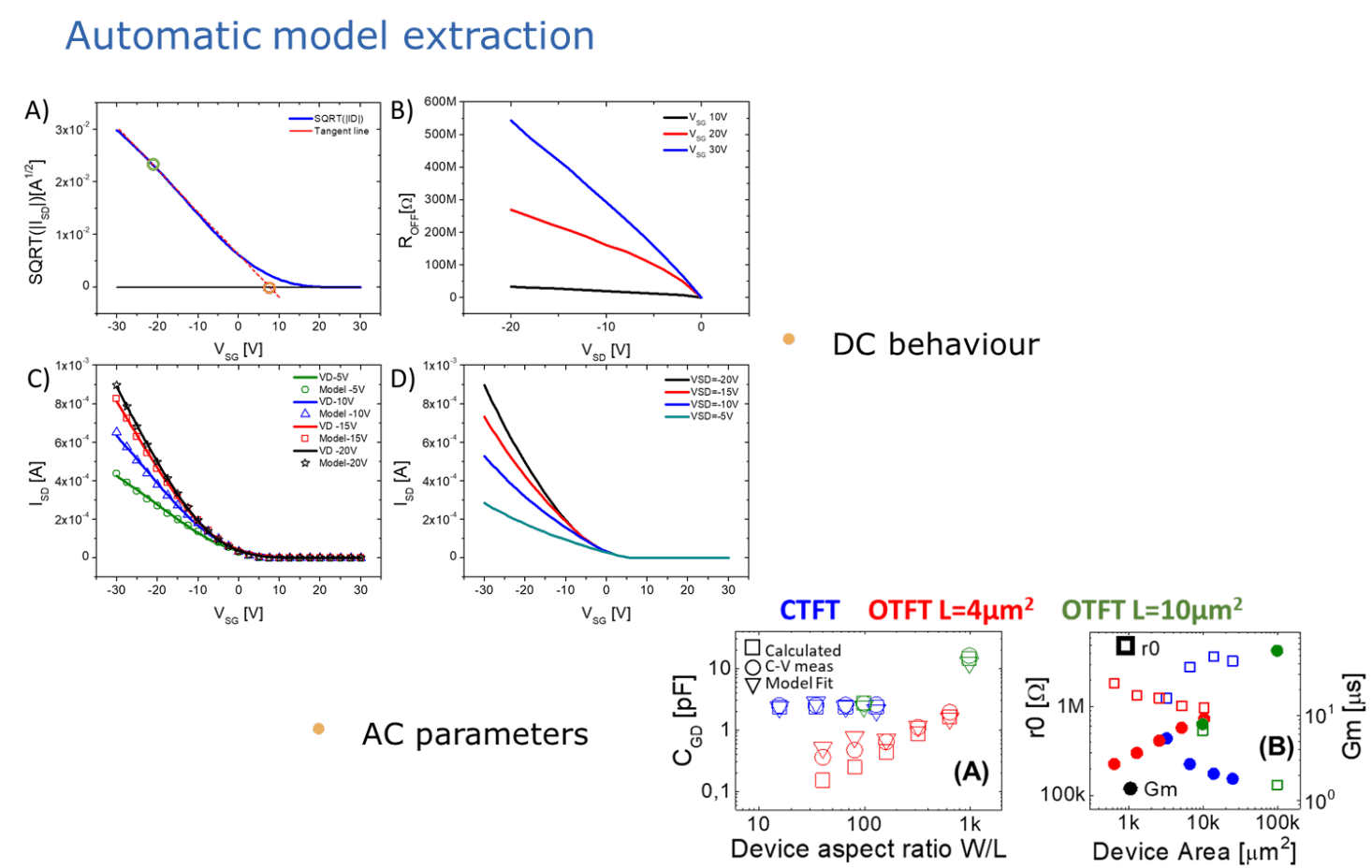
With all the data extracted, the model generation setup extracts and adjusts the model to fit to the device behaviour, allowing accumulated error lower than 0.2%. Furthermore, in the setup methodology the capacitance study allows the extraction of the capacitance value of multiple dimensions and architectures for AC parameters for model implementation.
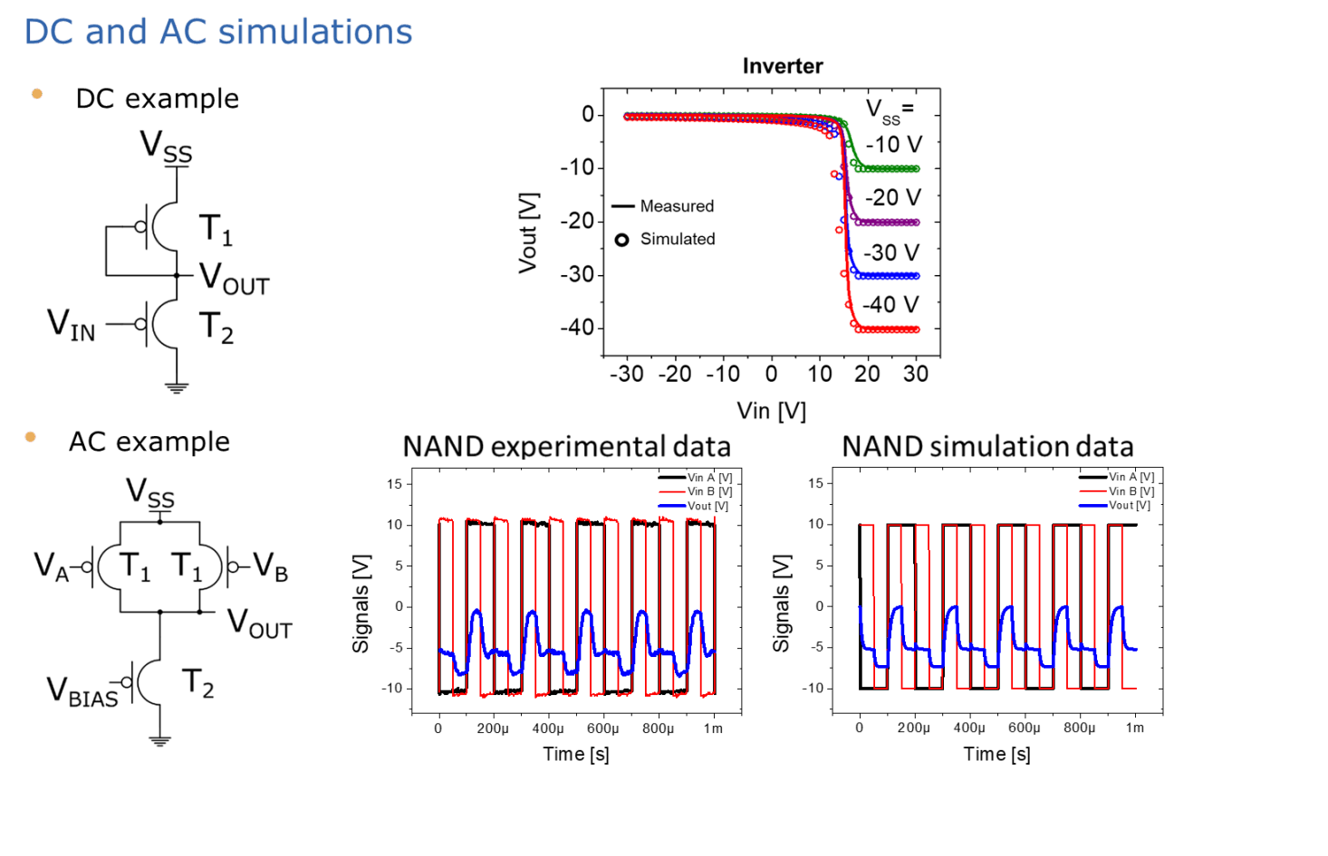
Circuit simulation
Circuit simulations of the model are done using Cadence Virtuoso, taking advantage of the tool’s full potential. Multiple DC or AC circuits can be implemented to accurately predict the response of the desired circuit.
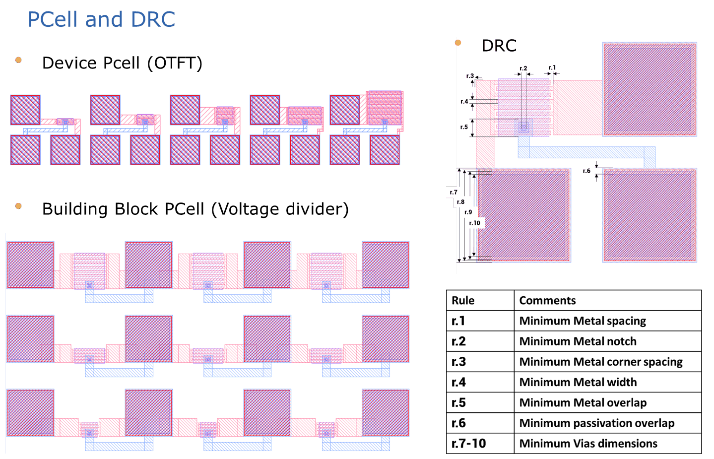
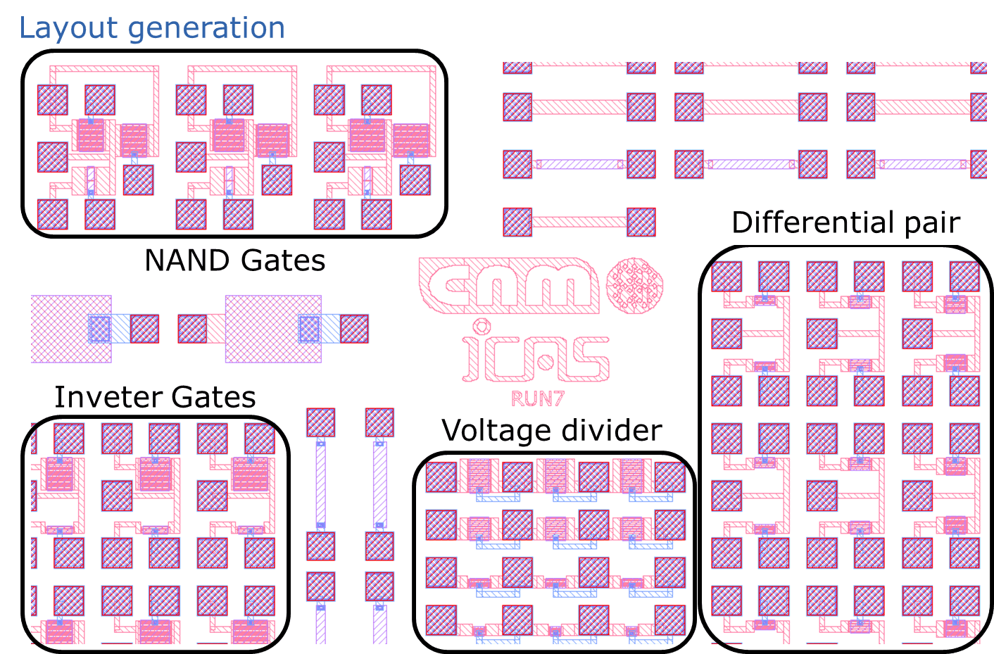
Layout design
In the layout step, the use of PCells allows fast and reliable design. DRC, ERC and LVS are also implemented to identify and fix any possible errors.
A. Arnal; C. Martínez-Domingo; S. Ogier; L. Terés; E. Ramon. Monotype organic dual threshold voltage using different OTFT geometries. Crystals. 9 - 7, 2019.http://dx.doi.org/10.3390/cryst9070333
A. Arnal, A. Crespo-Yepes, E. Ramon, L. Teres, R. Rodriguez, and M. Nafria. DC characterization and fast small-signal parameter extraction of organic thin film transistors with different geometries. IEEE Electron Device Lett., vol. 41, no. 10, pp. 1–1, 2020. https://doi.org/10.1109/LED.2020.3021236
A. Arnal. Organic Thin Film Transistors: Modelling, Simulation and Circuit Design. Master thesis dissertation, Univ. Autonoma de Barcelona, Bellaterra, Catalonia-Spain 2017.